JE Evans, G Burwell, FC Langbein, SG Shermer, K Kalna. Dilute Magnetic Contact for a Spin GaN HEMT. Semiconductor and Integrated OptoElectronics Conference (SIOE) Conference, Cardiff, 16-18 April, 2019. [PDF]
Semiconductor CMOS nano-electronics is intensively seeking solutions for future digital applications. One of the most promising solutions to deliver a technological breakthrough is exploring electron spin in metals and semiconductors with applications from spin transistors to quantum sensors, and quantum computing. Spintronic applications rely on magnetic semiconductor materials with suitable properties. In particular, dilute magnetic semiconductors (DMS), such as Mn doped GaN, show the great promise of a high Curie temperature (220K–370K), exceeding room temperature, and a large concentration of holes. These are all the essential pre-requisites for operation of spin transistors in circuits.
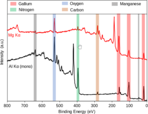
In this work, we dope an AlGaN/GaN heterostructure consisting of a GaN (2 nm) cap layer, an Al0.25Ga0.75N (25 nm) barrier, and a GaN (2 μm) substrate grown on a 6” Si wafer with Mn by sputtering deposition and thermal annealing to create a dilute magnetic semiconductor material following the process flow. While initial attempts resulted in the formation of a MnO surface layer, the SEM/XDS and XPS data suggest a diffusion of Mn into the GaN layer using thermal annealing at 900◦C for 7h with a concentration of 4.5% which is very close to the desired concentration of 5% needed for a DMS. The annealing temperature has to be below 1000◦ C since temperatures around 1000◦C result in significant damage to the 2DEG and diffusion of Al from the AlGaN layer.
![]() This work is licensed under a Creative Commons Attribution-NonCommercial-ShareAlike 4.0 International License.
This work is licensed under a Creative Commons Attribution-NonCommercial-ShareAlike 4.0 International License.

